As October begins, five companies—XinshiJia, Mailaide Microelectronics, Jingjia Semiconductor, Hangzhou Kaimu Photonics, and Eagle Semiconductor—have successively disclosed patent developments related to Micro-LED optical interconnect technology.
The patent applications cover several key areas, including Micro-LED co-packaged optics (CPO), Micro-LED transmitter and receiver pixel-drive circuits, gallium nitride (GaN)-based Micro-LED emitter arrays, and pluggable optical engines.
These innovations aim to improve optical coupling efficiency, transmitter-receiver matching, reliability, and maintainability in Micro-LED optical communications. They also address technical challenges such as thermal crosstalk between adjacent pixels, sidewall leakage currents, and non-radiative recombination in Micro-LED devices.
1. XinshiJia: Micro-LED-Based CPO Packaging Structure and Manufacturing Method
Anhui XinshiJia Semiconductor Display Technology Co., Ltd. has a patent application titled “A Micro-LED-Based CPO Packaging Structure and Manufacturing Method” that has entered the publication stage during patent examination.
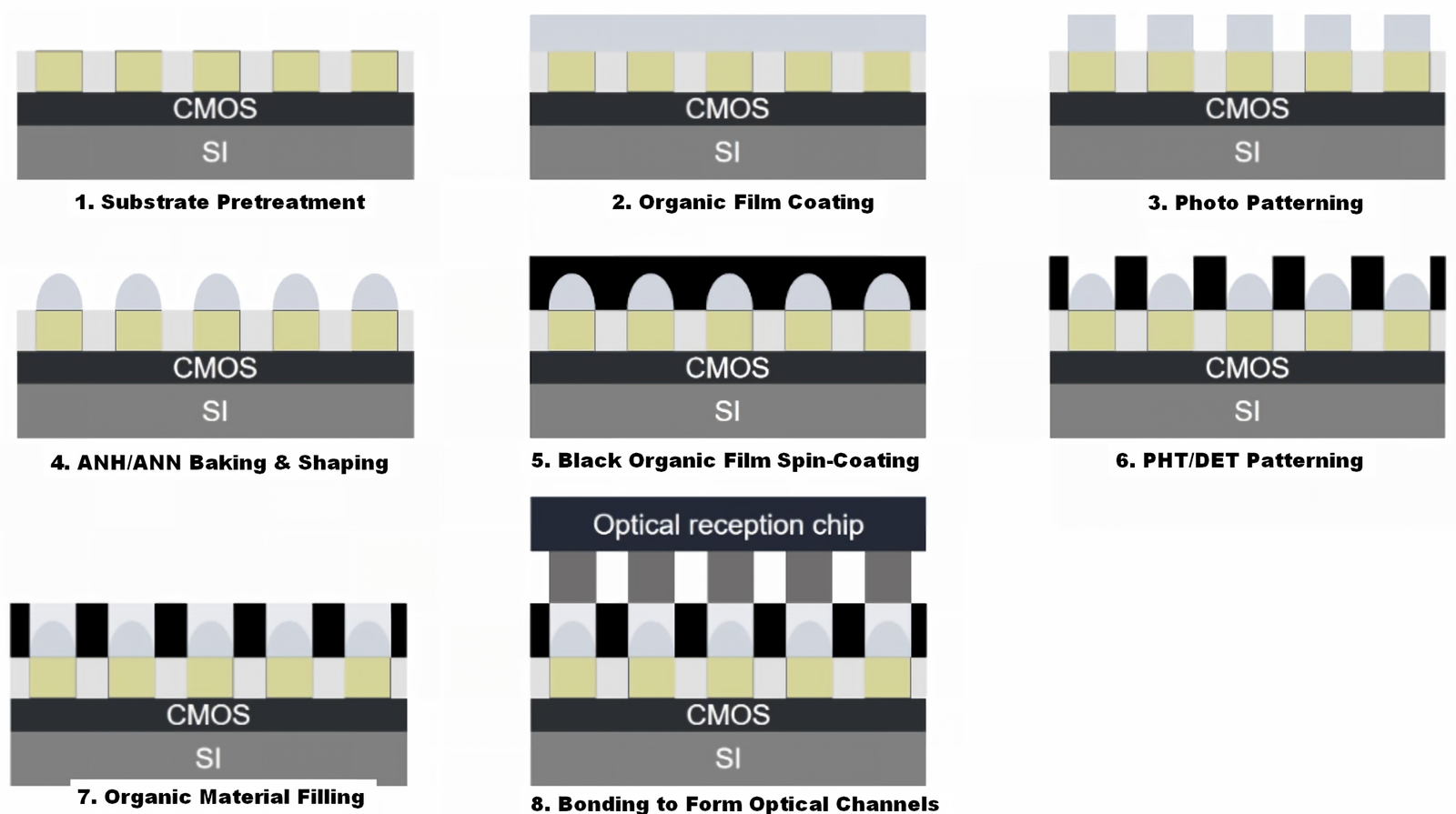
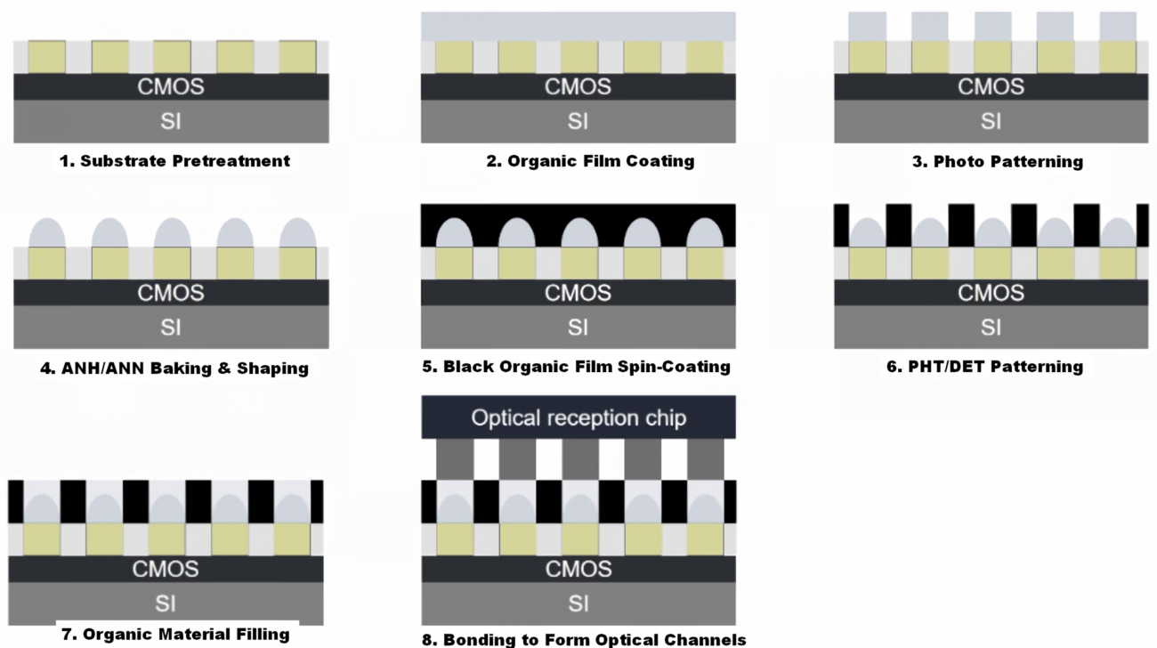
The invention relates to semiconductor optoelectronic packaging. Its proposed structure consists of multiple layers arranged from top to bottom: a fiber-coupling alignment layer, a microlens array layer, an optical buffer adhesive layer, a Micro-LED array layer, a CMOS driver substrate, and a thermal management and protection layer.
The microlens array contains multiple microlenses arranged in an array, with each microlens corresponding to an individual Micro-LED. Optical isolation barriers are positioned between adjacent microlenses, while a transparent optical buffer adhesive layer sits between the microlens array and the Micro-LED array.
By integrating pixel-level plano-convex microlenses, the design provides one-to-one optical matching between each Micro-LED and its corresponding lens. This helps concentrate widely diverging light into the acceptance angle of the optical fiber, significantly improving optical coupling efficiency.
2. Mailaide Microelectronics: Micro-LED Transmitter and Receiver Pixel-Drive Circuit for Optical Communications
On October 9, Mailaide Microelectronics Technology (Wuxi) Co., Ltd. announced the publication of its patent application titled “A Micro-LED Transmitter and Receiver Pixel-Drive Circuit for Optical Communications.”
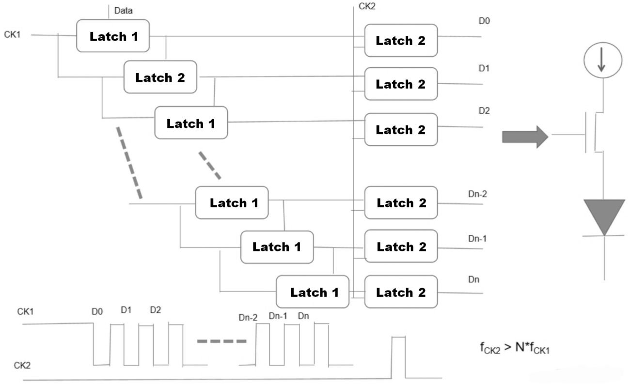
The invention focuses on optical communications, Micro-LED displays, and high-speed optoelectronic signal transmission. Its proposed circuit integrates a two-stage cascaded latch structure, multiple pairs of transmitter-side pixel circuits, and a receiver-side pixel decoding module.
The two-stage latch structure consists of a first-stage serial latch unit and a second-stage parallel latch unit.
The design establishes a complete optical communication system that integrates data latching, differential modulation, optical signal transmission, optoelectronic conversion, voltage comparison, and data decoding.
Transmitter and receiver pixel circuits can be paired on a one-to-one basis. On the receiving side, a Micro-LED pixel circuit is used directly as an optical sensing element, while a voltage comparator performs data decoding. This architecture eliminates the need for additional decoders or signal-conditioning circuits.
The approach is designed to improve transmitter-receiver matching and overall system integration, making it suitable for high-speed, parallel, short-distance optical communication applications.
3. Jingjia Semiconductor: GaN-Based Micro-LED Emitter Array with a Composite Heat-Dissipation Structure
Shandong Jingjia Semiconductor Co., Ltd. has a patent application titled “A GaN-Based Micro-LED Emitter Array with a Composite Heat-Dissipation Structure for Optical Interconnects and Its Manufacturing Method” that has entered the publication stage during examination.
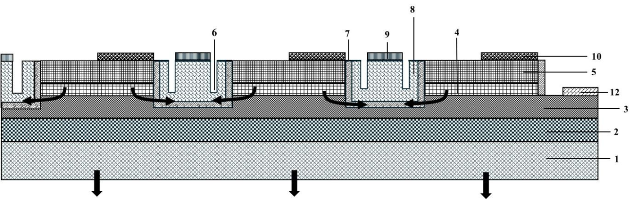
The invention relates to semiconductor light-emitting devices. The proposed emitter array consists of a single-crystal gallium nitride (GaN) substrate, a GaN homoepitaxial buffer layer, and an n-type GaN layer arranged from bottom to top.
The n-type GaN layer incorporates an array of Micro-LED emitting mesas and a common n-type electrode. Multiple spaces are formed between adjacent emitting mesas.
The sidewalls of each Micro-LED mesa, along with the bottoms of the spaces between mesas, are covered with an aluminum nitride (AlN) passivation layer. An AlN thermal-conductive layer fills the spaces outside the passivation layer, while a metal heat-dissipation layer is placed on top.
This structure enables electrical drive signals to be converted into optical signals emitted through the light-output windows. More importantly, the composite thermal management design is intended to reduce thermal crosstalk between adjacent pixels in the Micro-LED array.
The AlN passivation structure also helps reduce sidewall leakage currents and non-radiative recombination, addressing important challenges in Micro-LED device performance and reliability.
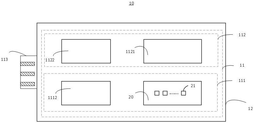
4. Hangzhou Kaimu Photonics and Eagle Semiconductor: High-Density Pluggable Optical Engine
On October 9, Hangzhou Kaimu Photonics Technology Co., Ltd. and Zhejiang Eagle Semiconductor Technology Co., Ltd. disclosed a patent application titled “A High-Density Pluggable Optical Engine.”
The proposed optical engine incorporates an optical transmitter unit containing laser chips. Each laser chip includes at least one Micro-VCSEL emitter, with a lateral feature size of less than 100 micrometers.
Micro-VCSEL emitters offer several advantages, including high per-channel bandwidth, compact dimensions, circularly symmetric beam profiles, small divergence angles, high integration density, and compatibility with flip-chip bonding and packaging.
When used as light sources in high-speed optical interconnects for data centers, Micro-VCSEL technology can enable more high-speed optical channels to be integrated within the same package footprint. This combines compact form factors with high interconnect bandwidth, supporting applications that require miniaturization, high density, low power consumption, and ultra-high-speed data transmission.
Another key feature is the integration of complex optical engine functions into a hot-pluggable module that can interface with external systems. This modular approach offers greater flexibility and convenience while improving the reliability and maintainability of optical interconnect systems.
Conclusion: Micro-LED Optical Interconnects Move Toward Higher Integration and Reliability
These patent developments highlight several important directions in Micro-LED optical interconnect technology.
- Higher optical coupling efficiency: Pixel-level microlens arrays help direct emitted light into optical fibers more efficiently.
- Improved transmitter-receiver integration: Integrated pixel-drive and decoding circuits support high-speed, short-distance optical communications.
- Better thermal management and device reliability: Composite heat-dissipation structures help mitigate thermal crosstalk, sidewall leakage, and non-radiative recombination.
- Higher-density, more maintainable optical systems: Compact Micro-VCSEL emitters and hot-pluggable optical engines support scalable, high-bandwidth interconnects for data centers.
As demand for high-bandwidth data transmission continues to grow, driven by AI computing and increasingly demanding data-center workloads, Micro-LED and related optical interconnect technologies are attracting attention as potential solutions for highly integrated, energy-efficient communication systems.
Further development in optoelectronic integration, thermal management, and advanced packaging will be important to translating these innovations into practical applications.
#Micro-LED optical interconnects