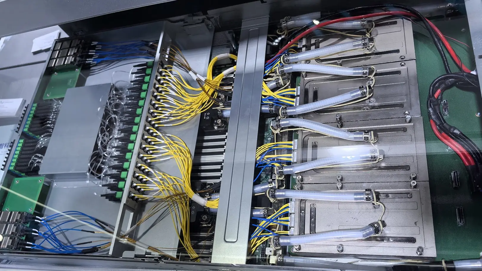
As data center networks move toward 224G-per-lane speeds, the traditional way of connecting a switch chip to an optical module is running out of headroom. In a conventional architecture, the optical module plugs into the switch faceplate, and electrical signals travel ten or more centimeters across the PCB before reaching the optics. The longer the distance and the higher the rate, the worse the insertion loss — and the higher the power consumption.
Two advanced interconnect approaches are competing to close that distance: CPO (Co-Packaged Optics) and NPO (Near-Package Optics, sometimes called near-packaged or semi-co-packaged optics). Understanding the difference matters for anyone building optical modules, switch platforms, or the packaging processes behind them.
What Is NPO?
NPO moves the optical engine off the faceplate and places it on the same PCB as the switch chip, just a few centimeters away (roughly 2–5 cm instead of 10+ cm).
That shorter distance delivers two major benefits:
1. Insertion loss drops dramatically. Typical pluggable-channel insertion loss of 22–26 dB falls to around 7–9 dB. At 224G per lane, NPO architectures can hold total insertion loss near 10 dB — comfortably better than pluggable designs.
2. The DSP can be removed. With less loss to compensate, the signal stays within the tolerance range of analog circuits. The switch chip’s SerDes can drive the laser linearly, and the receiver needs only a transimpedance amplifier (TIA). The digital signal processing stage — traditionally the most power-hungry part of a module — is eliminated entirely. This is known as linear direct drive, and it cuts both power consumption and cost.
The trade-off: the optical engine must now be designed into the PCB layout, changing how switch boards are engineered.
Crucially, though, an NPO optical engine remains a modular, replaceable unit. This is the fundamental distinction from CPO — and the reason NPO can reuse today’s mature pluggable-module production lines and supply chain.
NPO vs CPO: The Real Difference Is the Optics-Electronics Boundary
NPO is often mistaken for a “budget CPO.” In reality, the two differ not in a performance number but in where the boundary between electronics and photonics sits:
- NPO: the optical engine and the switch chip share the same board but live in separate packages — “same board, different shells.”
- CPO: electronics and photonics are fused. The optical engine and the switch chip are integrated on the same silicon interposer inside one package, using 2.5D/3D advanced packaging (such as CoWoS-class processes and hybrid bonding).
Every practical consequence flows from that boundary:
| Aspect | NPO (Near-Package Optics) | CPO (Co-Packaged Optics) |
| Optics-chip relationship | Same PCB, separate packages | One package; optics + switch chip on silicon interposer |
| Insertion loss | ~10 dB at 224G/lane | Lower still; 1.6T port power can reach ~9 W |
| Power savings vs pluggable | 30–40% | Over 50% |
| Serviceability | Module-level replacement | Optics soldered in; a single fault can require replacing the entire substrate or system |
| Yield control | High (mature module processes) | Very difficult (optical-electrical bonding at package level) |
| Supply chain | Reuses pluggable-module lines and ecosystem | Depends on top-tier advanced packaging capacity |
| Best described as | Pragmatic near-term path | Ultimate long-term destination |
CPO offers the higher ceiling — roughly half the power of traditional solutions at 1.6T — at the cost of soldered-in optics, hard yield control, and dependence on leading-edge 2.5D/3D packaging capacity. To date, volume CPO switch production has been achieved by only one player, and most of the industry cannot yet replicate it.
NPO is less extreme, but at 200G/lane its gap to CPO is under 5% — while preserving module-level replaceability, high yields, stable supply chains, and reuse of existing production lines.
Why NPO Is Winning Near-Term Momentum
Industry analysis points to 2026–2027 as the window in which NPO becomes the highest-certainty growth area for optical interconnect, particularly in the Chinese market, where it follows a “define the standard, adapt the line, validate with cloud operators” path:
- Standards: In July 2026, Huawei and more than 20 partner organizations launched the OPEN NPO initiative, releasing China’s first NPO multi-source agreement (MSA).
- Products: HGTECH announced the world’s first 3.2T NPO; Accelink demonstrated the world’s first 3.2T silicon photonics single-mode NPO module at OFC 2026; Eoptolink showcased 6.4T silicon photonics NPO and 12.8T XPO samples. Innolight has named NPO a next-generation core direction, with sampling expected in 2026 and mass production in 2027.
- Demand: Cloud operators are the anchor buyers. Alibaba has completed beta testing of 3.2T NPO with data center pilots in Q3; Tencent has completed reliability verification with pilots planned for Q4.
For module makers in Southeast Asia and beyond, the message is clear: NPO-class engines will flow through packaging and assembly lines at scale, and the lines that handle them must meet semiconductor-grade process standards.
What NPO and CPO Mean for Assembly and Cleaning Processes
Here is where optics packaging converges with a topic we cover often: precision cleaning.
NPO brings semiconductor-grade packaging discipline to module lines. An NPO optical engine is assembled with die attach, wire bonding or flip-chip interconnects, and precision submounts — the same process families used in IC packaging. Flux residues, die-attach outgassing, and contamination that were tolerable in a faceplate-pluggable world become reliability risks inside an engine sitting centimeters from a switch ASIC:
- Flux residue near optical paths and bond pads can absorb moisture, cause leakage or corrosion, and degrade long-term reliability — the same failure mechanisms seen in BGA and flip-chip packages.
- Cleaning before bonding and encapsulation (optical coupling adhesives, underfills) is critical; residue at bonding interfaces causes delamination and optical misalignment over thermal cycling.
- Low-standoff, fine-pitch geometries inside optical engines demand the same agitation technologies used in semiconductor packaging cleaning: spray, ultrasonic, jet flow, and controlled drying to avoid water marks on optical surfaces.
CPO raises the bar further. Hybrid bonding and silicon interposer processes require particle-level cleanliness and validated ionic contamination control — cleaning is no longer a post-solder step but a yield-critical process gate.
Manufacturers positioning for the NPO/CPO transition should audit their cleaning capability now: compatibility with water-based and solvent cleaning agents, coverage of low-standoff gaps, vacuum drying for moisture-sensitive optics, and cleanliness verification with ion contamination testing.
The Takeaway
NPO and CPO are not rivals so much as two points on the same journey — moving photons closer to silicon. CPO defines the destination; NPO is the practical road that reuses today’s module lines to get there first. For optical module and packaging manufacturers, NPO’s 2026–2027 ramp-up is an opportunity — but only for lines ready to operate at semiconductor packaging process standards, cleanliness included.
ACTSPRAY, a high-tech enterprise in Chang’an Town, Dongguan, China, specializes in cleaning process R&D and cleaning equipment manufacturing for the microelectronics industry — including optical module and sensor packaging applications. Our machines master spray, ultrasonic, jet flow, vacuum and gas phase technologies, and we support rapid customized equipment development with full-cycle technical support.
Building NPO or optical engine assembly capability? Contact our engineering team to discuss a cleaning process matched to your package design.
–Industry trends referenced from public reports, October 2026.